
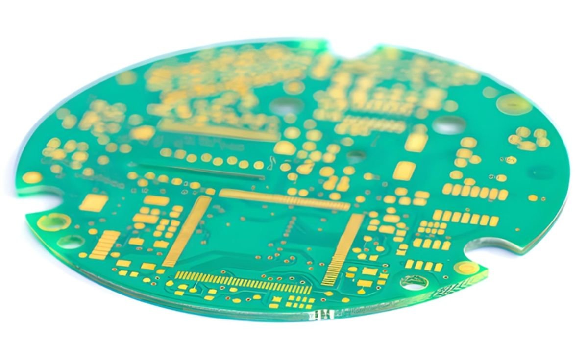
As modern electronic devices become more powerful and compact, circuit board technology has evolved to support increasing functionality within smaller spaces. Traditional single-sided and double-sided PCBs are often insufficient for advanced electronic systems that require high component density, faster signal transmission, and improved reliability. This is where the Multilayer PCB plays a crucial role.
Multilayer PCBs have become the foundation of modern electronics, enabling the development of sophisticated products such as smartphones, medical equipment, automotive control systems, industrial automation devices, and telecommunications infrastructure. Their ability to integrate complex circuits into a compact design makes them one of the most widely used PCB technologies today.
What Is a Multilayer PCB?
A Multilayer PCB is a printed circuit board that consists of three or more conductive copper layers separated by insulating materials and bonded together through a lamination process. Unlike single-sided or double-sided PCBs, multilayer boards allow designers to route signals, power, and ground connections across multiple layers, significantly increasing circuit density.
The number of layers can vary depending on the complexity of the application. Common configurations include 4-layer, 6-layer, 8-layer, and 12-layer PCBs, while highly advanced systems may use 20 or more layers.
By stacking multiple conductive layers within a single board, engineers can create compact and highly functional electronic systems without sacrificing performance.
Structure of a Multilayer PCB
The structure of a Multilayer PCB is carefully engineered to ensure optimal electrical performance and mechanical reliability.
A typical multilayer PCB consists of alternating layers of copper foil and dielectric materials. The outer layers are used for component placement and signal routing, while the inner layers often serve as dedicated power and ground planes.
The dielectric layers provide electrical insulation between copper layers while maintaining structural integrity. These layers are usually made from FR4 epoxy fiberglass or other specialized materials depending on the application.
Vias are used to establish electrical connections between different layers. Through-hole vias, blind vias, and buried vias enable signals to travel throughout the board while maintaining efficient routing.
This layered construction allows designers to separate high-speed signals, power distribution, and grounding functions, resulting in improved overall performance.
Types of Multilayer PCBs
Different types of Multilayer PCB designs are available to meet various application requirements.
Standard multilayer PCBs are commonly used in consumer electronics and industrial equipment. These boards typically contain four to twelve layers.
High-density interconnect (HDI) multilayer PCBs use microvias and fine traces to achieve extremely high circuit density. They are widely used in smartphones, tablets, and wearable devices.
Rigid multilayer PCBs provide excellent mechanical stability and are suitable for applications that require durability and long-term reliability.
Rigid-flex multilayer PCBs combine rigid and flexible sections, enabling compact and space-saving designs for aerospace, medical, and automotive systems.
The selection of a multilayer PCB type depends on performance requirements, design complexity, and budget considerations.
Manufacturing Process of Multilayer PCBs
The manufacturing of a Multilayer PCB involves several complex steps that require precision and advanced equipment.
The process begins with creating the inner layer circuits. Copper-clad laminates are coated with photoresist, exposed to ultraviolet light through a circuit pattern, and then etched to form the desired traces.
After inspection, the inner layers are stacked with prepreg insulation materials and copper foils. The stack is subjected to high temperature and pressure during the lamination process, bonding all layers into a single structure.
Once laminated, drilling is performed to create vias and component holes. The holes are then plated with copper to establish electrical connections between layers.
The outer layers are patterned and etched to create the final circuit layout. A solder mask is applied to protect the copper traces, followed by the addition of silkscreen markings for component identification.
Finally, the board undergoes comprehensive electrical testing and quality inspection before shipment.
Advantages of Multilayer PCBs
One of the most significant advantages of a Multilayer PCB is its ability to support highly complex circuits within a compact footprint. This allows manufacturers to develop smaller and more powerful electronic devices.
Improved signal integrity is another major benefit. Dedicated power and ground planes help reduce electromagnetic interference and signal noise, resulting in more stable performance.
Multilayer PCBs also offer enhanced reliability. Their laminated construction provides excellent mechanical strength and resistance to environmental stress.
The increased layer count enables more efficient routing, reducing the need for external wiring and connectors. This simplifies assembly and improves overall system reliability.
Additionally, multilayer PCBs support high-speed signal transmission, making them ideal for advanced communication and computing applications.
Applications of Multilayer PCBs
The versatility of Multilayer PCB technology makes it essential across numerous industries.
In consumer electronics, multilayer PCBs are used in smartphones, tablets, laptops, gaming consoles, and smart home devices. Their compact design supports the integration of advanced features within small products.
The automotive industry relies heavily on multilayer PCBs for engine control units, infotainment systems, battery management systems, and advanced driver-assistance systems.
Medical equipment such as MRI scanners, patient monitoring systems, and diagnostic devices utilize multilayer PCBs to achieve high performance and reliability.
Telecommunications infrastructure, including routers, switches, servers, and 5G base stations, depends on multilayer PCB technology to manage high-speed data transmission.
Industrial automation systems, robotics, aerospace equipment, and defense applications also benefit from the durability and performance offered by multilayer PCBs.
Design Considerations for Multilayer PCBs
Designing a Multilayer PCB requires careful planning to achieve optimal performance.
Layer stack-up design is one of the most important considerations. Proper placement of signal, power, and ground layers helps minimize interference and improve signal integrity.
Controlled impedance is critical for high-speed circuits. Designers must carefully calculate trace widths, spacing, and dielectric properties to ensure reliable signal transmission.
Thermal management is another important factor. High-density boards can generate significant heat, requiring proper heat dissipation strategies.
Via placement and routing must be optimized to minimize signal loss and maintain manufacturability.
Engineers must also consider manufacturing capabilities and tolerances to ensure that the design can be produced efficiently and cost-effectively.
Challenges of Multilayer PCB Manufacturing
Although Multilayer PCB technology offers numerous benefits, it also presents certain challenges.
The manufacturing process is more complex than that of single-sided or double-sided boards, requiring advanced equipment and strict quality control.
As the number of layers increases, alignment and lamination become more critical. Even minor deviations can impact performance and reliability.
Repair and rework are also more difficult due to the board’s layered structure.
Additionally, multilayer PCBs generally have higher production costs due to increased material usage and manufacturing complexity.
Despite these challenges, their performance advantages often justify the investment for advanced electronic applications.
Conclusion
The Multilayer PCB has become an indispensable technology in modern electronics, enabling compact designs, improved signal integrity, and enhanced functionality. Its ability to integrate multiple conductive layers within a single board makes it the preferred choice for industries ranging from consumer electronics and telecommunications to automotive, medical, and aerospace applications.
As electronic systems continue to become more sophisticated, the demand for advanced multilayer PCB solutions will only increase. Companies seeking reliable, high-performance circuit boards often partner with an experienced Multilayer PCB manufacturer to ensure superior quality, precision manufacturing, and long-term product reliability.
[…] helping clinicians determine the degree of stenosis and plan appropriate treatment. Just as multilayer PCB structures rely on precise layering and imaging to ensure signal integrity, modern vascular diagnostics depend on layered imaging technologies to accurately map arterial […]